Press Release - L&K’s Hefei Changxin Project
date:2020-07-20 browser:177
Hefei Changxin 12-inches Memory Wafer Manufacturing Base Project was founded in June, 2016. With a total investment of about 150 billion Yuan, the project is an industrial project with the largest single investment in Anhui Province. It will be built into the first and the largest self-developed DRAM manufacturing base in China and also the fourth manufacturer adopting 20 nanometers or lower technique for DRAM in the world. The design production capacity of the first phase is 120,000 wafer per month.
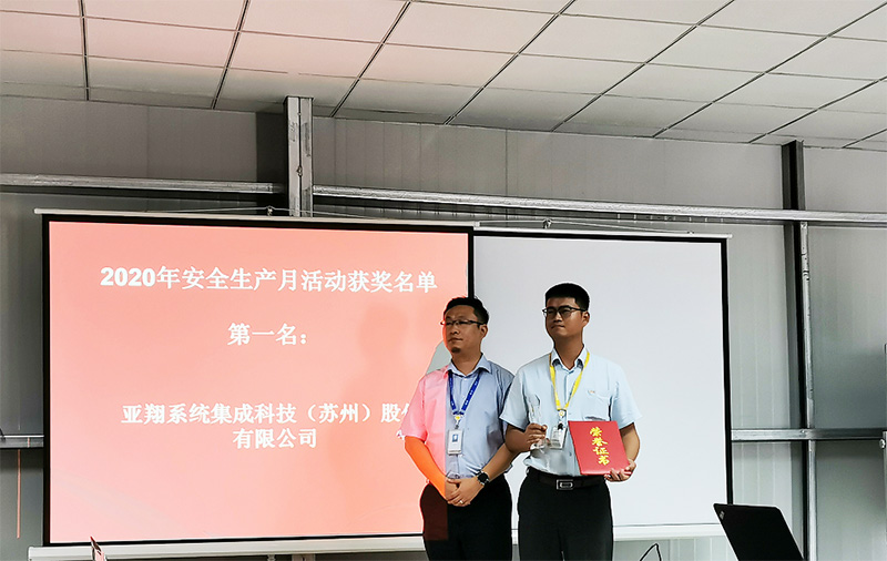
In the construction of Hefei Changxin project, the project management team of L&K has been working hard without complaint all the time during the implementation process. They have been diligent and actively overcome the on-site difficulties, and their safety management has been recognized by the owner.
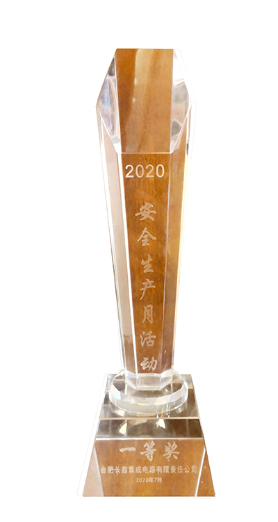
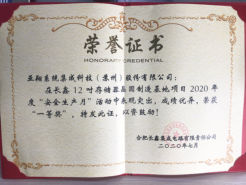
The owners of Changxin Integration and IT Electronics Eleventh Design & Research Institute Scientific and Technological Engineering Corporation Limited (“EDRI”) conducted an annual evaluation among 20 professional subcontractors on Production Safety Month in 2020. The project team of L&K won the first prize in the evaluation, and won the certificate and trophy of “ First Prize for Annual Production Safety Month Evaluation in 2020” awarded by the owner of Changxin Integration.